ASIC Transistor Layout - CMOS Logic Design Details

ASIC Transistor Layout - CMOS Logic Design
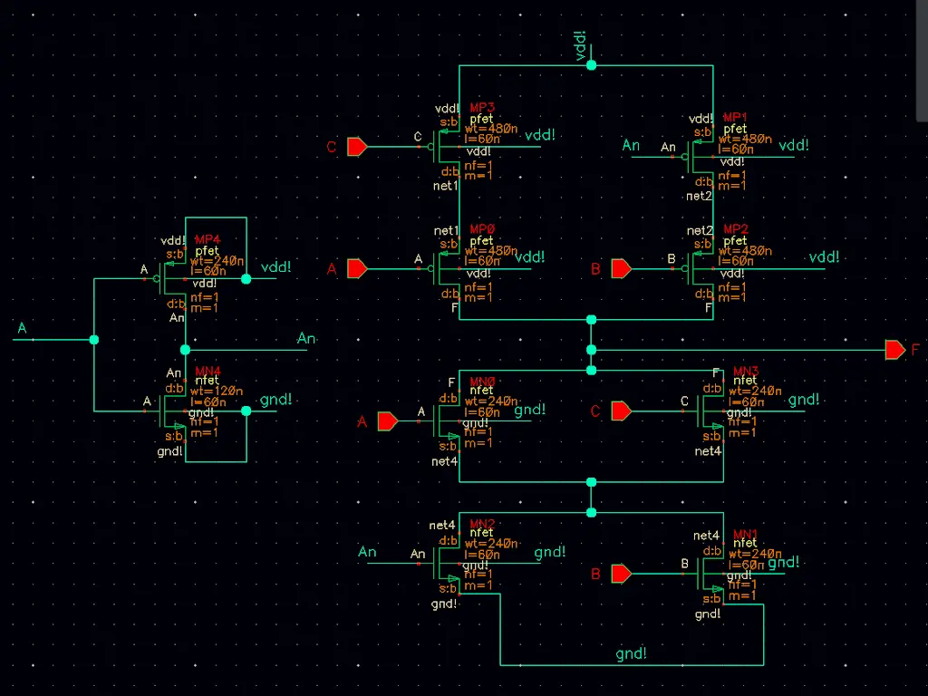
This project focuses on the design and implementation of a complimentary static CMOS circuit for the logic function: f = A'C' + BA' + AB'. The goal was to minimize transistor usage while ensuring efficient functionality through careful circuit optimization and layout techniques. Key deliverables included schematic design, compact layout creation, simulation, and performance analysis.
Objectives
- Minimize transistor count by simplifying the logic function using Karnaugh Maps and Boolean algebra.
- Develop a compact CMOS layout with efficient source/drain sharing and minimal interconnect lengths.
- Evaluate performance through simulations with varying load capacitances.
Project Process
- Schematic Design: Transistor widths were chosen to balance performance and minimize resistance variations, with NMOS/PMOS lengths fixed at 60nm.
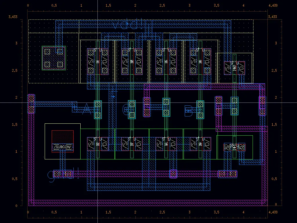
- CMOS Layout Implementation: A compact layout was created using a 3.433 μm × 4.439 μm area (15.239 μm²), utilizing source/drain sharing to reduce parasitic effects.
- Design Rule and Verification Checks: Passed DRC, LVS, and PEX checks to ensure the layout met design and fabrication constraints.
- Simulation Results: - Achieved a maximum frequency of 5 GHz with a 0.5 fF load and 1.67 GHz with a 15 fF load. - Post-layout simulations showed slower rise/fall times due to parasitic capacitances.
Conclusion and Future Improvements
The project demonstrated speeds of 5 GHz (0.5 fF load) and 1.67 GHz (15 fF load), highlighting the impact of load capacitance on performance. Future improvements could focus on reducing parasitic capacitances through layout optimization and fine-tuning transistor dimensions to enhance speed under higher loads.
Project Information
- Category: Design/Hardware
- Client: Rensselaer Polytechnic Institute
- Project date: 28 November, 2024
- Project PDF: Download MEMO