Pipelined and Parrellelized FPGA 102 Tap FIR Filter
High-Performance 102-Tap FIR Filter with Pipelined and Parallelized Architectures
This project designs and implements a low-pass FIR filter with 102 taps, targeting FPGA platforms. The filter achieves a transition region of 0.2π–0.23π rad/sample, >80 dB stopband attenuation, and robust noise suppression for a 1 kHz sine wave input. Leveraging MATLAB, Python, and Verilog, the design explores pipelined, parallel (L=2/L=3), and hybrid architectures to optimize throughput, area, and power efficiency.
Objectives
- Design a 102-tap FIR filter with MATLAB, ensuring >80 dB stopband attenuation
- Quantize coefficients to 32-bit fixed-point and manage arithmetic overflow
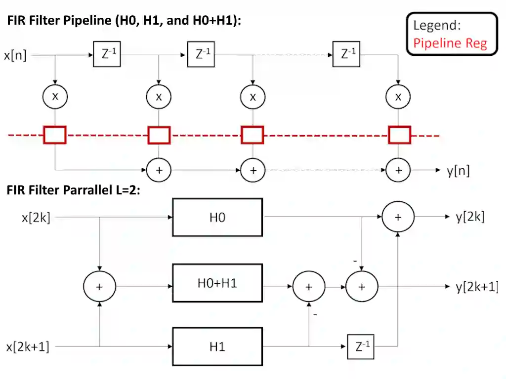
- Implement four architectures: Traditional, Pipelined, L=2/L=3 Parallel, and Combined Pipelined & L=3
- Analyze hardware metrics (area, frequency, power) across architectures
- Validate noise removal using ModelSim and MATLAB frequency response analysis
Project Process
-
MATLAB Filter Design & Quantization:
- Generated ideal coefficients using MATLAB’s FIR design tools
- Quantized coefficients to 32-bit signed format with scaling to prevent overflow
- Analyzed frequency response deviations post-quantization (<1 dB ripple in passband)
-
Architecture Implementation:
- Traditional: Direct-form MAC structure with 102 taps
- Pipelined: Inserted pipeline stages in MAC units to reduce critical path delays
- Parallel L=2/L=3: Split coefficients into sub-filters via Python-based polyphase decomposition
- Combined Pipelined & L=3: Merged pipelining with parallel processing for maximum throughput
-
Hardware Synthesis:
- Synthesized designs using Synopsys Design Compiler (45nm technology)
- Compared area utilization: 811 cells (Pipelined) vs 13,831 cells (Combined L=3)
- Achieved 47 kHz clock frequency with >21,000 ns setup slack across all designs
- Optimized power consumption: 8.22 μW leakage (Pipelined) vs 351.29 μW total (Combined)
-
Validation & Analysis:
- Verified noise removal using ModelSim with 16-bit noisy sine wave input
- Confirmed stopband attenuation >80 dB post-quantization via MATLAB analysis
- Demonstrated 2.3x throughput improvement in L=3 vs Traditional architecture
Conclusion and Future Improvements
The pipelined architecture achieved optimal balance between area (811 cells) and power (8.22 μW), while the combined L=3 design maximized throughput at higher resource costs. Future enhancements could explore higher-order parallelization (L=4+), adaptive coefficient tuning, or ASIC implementation for ultra-low-power edge applications. The modular Verilog codebase and automated Python/MATLAB workflows provide a scalable foundation for real-time DSP systems.
Project Information
- Category: Digital Signal Processing / VLSI Design
- Client: Rensselaer Polytechnic Institute
- Project Date: March 14, 2025
- GitHub Repository: View Implementation